Hostname: page-component-848d4c4894-wg55d Total loading time: 0 Render date: 2024-06-02T08:37:24.783Z Has data issue: false hasContentIssue false

Defect analysis of star defects in GaN thin films grown on HVPE GaN substrates

Published online by Cambridge University Press:  30 July 2021

Tim Ruggles
Affiliation:
Sandia National Laboratories, Albuquerque, New Mexico, United States
Julia Deitz
Affiliation:
Sandia National Laboratory, United States
Andrew Allerman
Affiliation:
Sandia National Laboratories, Albuquerque, New Mexico, United States
C. Barry Carter
Affiliation:
University of Connecticut, Connecticut, United States
Joseph Michael
Affiliation:
Sandia National Laboratory, United States

Abstract

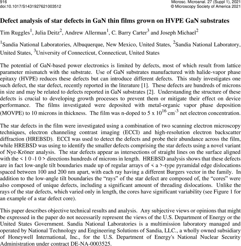
Image of the first page of this content. For PDF version, please use the ‘Save PDF’ preceeding this image.'
Type
Defects in Materials: How We See and Understand Them
Copyright
Copyright © The Author(s), 2021. Published by Cambridge University Press on behalf of the Microscopy Society of America

References

Ruggles, T., Deitz, J., Allerman, A., Carter, C.B., Michael, J., 2021, Identification of star defects in gallium nitride with HREBSD and ECCI. Microscopy & Microanalysis, in pressGoogle Scholar
Raghothamachar, B., Liu, Y., Peng, H., Ailihuamaer, T., Dudley, M., Shahedipour-Sandvik, F.S., Jones, K.A., Armstrong, A., Allerman, A.A., Han, J., et al. , 2020. X-ray topography characterization of gallium nitride substrates for power device development. Journal of Crystal Growth , 125709.Google Scholar